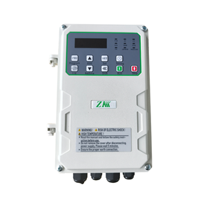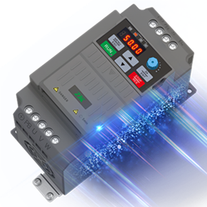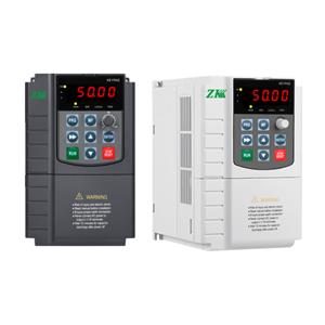
Optimizing Power Modules for VFDs
Frequency converters (FCs), the workhorses transforming electrical power for applications from industrial motor drives to renewable energy integration, rely fundamentally on power modules. Power modules, typically housing Insulated Gate Bipolar Transistors (IGBTs) or Silicon Carbide (SiC) MOSFETs, perform the critical switching operations. Optimization of power modules is paramount, requiring a deep understanding of both steady-state and transient performance characteristics and the intricate, often competing, trade-offs involved.
The Crucial Duality: Steady-State vs. Transient
· Steady-State Performance: This refers to power modules' behavior under continuous, stable operating conditions – constant load, fixed output frequency/voltage. Key metrics here are:
o Conduction Losses: Power dissipated as heat when the semiconductor device is fully "on" (saturated). This is primarily determined by the semiconductor device's on-state resistance (R_ds(on) for MOSFETs) or collector-emitter saturation voltage (V_ce(sat) for IGBTs). Lower conduction losses directly translate to higher overall system efficiency and reduced cooling requirements.
o Thermal Management: Efficient heat dissipation is critical. Steady-state losses generate continuous heat, demanding optimized thermal interfaces (thermal paste, pads), heatsink design, and cooling methods (forced air, liquid) to keep junction temperatures within safe limits, preventing degradation and failure of power modules.
o Output Waveform Quality: Low harmonic distortion and precise voltage/current control under steady load are essential for motor health and grid compatibility. This relates to the accuracy and stability of the switching control within power modules and the converter control loop.
· Transient Performance: This governs power modules' behavior during rapid changes – switching events (turning on/off), load transients (sudden motor start/stop), or input fluctuations. Key metrics include:
o Switching Losses: Energy dissipated during the turn-on and turn-off transitions themselves. This is influenced by the speed of the switching (dv/dt, di/dt), the semiconductor device's inherent capacitance, and the characteristics of the gate driver circuit. High switching frequencies (used to reduce output filter size and improve waveform quality) increase the cumulative impact of these losses.
o Switching Speed (dv/dt, di/dt): How rapidly voltage and current change during transitions. Faster switching reduces switching losses but increases electromagnetic interference (EMI) and stresses on power modules and connected components (e.g., motor windings, snubbers). Faster switching also increases the risk of phenomena like shoot-through (both upper and lower devices in a phase leg conducting simultaneously, causing a short circuit).
o Ruggedness: The ability of power modules to withstand abnormal conditions like short circuits, overvoltage spikes (e.g., from load dump or switching inductive loads), and overcurrent without failure. Ruggedness depends on semiconductor device structure, gate control robustness, and protective circuitry integration.
Optimizing Power Modules: Balancing the Scales
Optimizing power modules requires a holistic approach that addresses both operational states, often involving careful compromises:
1. Semiconductor Material & Structure:
o Silicon Carbide/Gallium Nitride vs. Silicon: Wide Bandgap semiconductor devices like silicon carbide MOSFETs offer revolutionary advantages. Silicon carbide MOSFETs exhibit significantly lower conduction losses (lower R_ds(on)) and dramatically lower switching losses compared to traditional silicon IGBTs. This allows for much higher switching frequencies, improving steady-state waveform quality and reducing passive component size (filters, capacitors), while simultaneously boosting overall efficiency in both steady-state and transient operation. Silicon carbide MOSFETs also tolerate higher junction temperatures.
o Semiconductor Device Design: Internal geometry (cell density, gate structure) influences R_ds(on), switching speed, and short-circuit withstand capability. Optimizing semiconductor device design involves complex trade-offs.
2. Gate Driver Circuit Design (Critical for Transients & Steady-State):
o Drive Strength & Speed: A powerful, low-impedance gate driver circuit is essential for fast switching (reducing transient switching losses). However, controllable speed is key. Intelligent gate driver circuits allow adjustment of turn-on/turn-off slew rates (dv/dt, di/dt) to find the sweet spot: minimize switching losses while managing EMI and voltage overshoot.
o Protection Features: Integrated desaturation detection, short-circuit protection, soft turn-off under fault conditions, and undervoltage lockout (UVLO) are vital for transient ruggedness and preventing catastrophic failure of power modules during faults.
o Isolation & Noise Immunity: Robust isolation between the control side (low voltage) and power side (high voltage) is non-negotiable for safety and reliable operation of power modules, especially during noisy switching transients.
3. Thermal Management & Packaging (Impacts Both States):
o Low Thermal Resistance: Minimizing the thermal resistance from the semiconductor junction to the heatsink (R_th(j-c), R_th(c-s)) is fundamental for managing heat generated by both conduction losses (steady-state) and switching losses (transient, but cumulative) within power modules. Advanced packaging for power modules uses direct copper bonding, silver sintering, and baseplates with high thermal conductivity.
o Reliable Interconnects: Bond wires and solder joints within power modules must withstand constant thermal cycling caused by load variations (transients) and the inherent heating/cooling from switching. Fatigue leads to increased resistance (higher conduction loss) and eventual failure of power modules. Ribbon bonding, clip bonding, or even leadframe designs improve reliability of interconnects.
o Cooling System Synergy: Design of power modules must facilitate efficient heat transfer to the chosen cooling solution (heatsink fins, cold plates).
4. Parasitic Minimization (Critical for Transients):
o Layout: Power loops (the physical path for high di/dt currents) must be as short and symmetric as possible within power modules and on the PCB. This minimizes parasitic inductance (L_par), which causes destructive voltage spikes (V_spike = L_par * di/dt) during switching transients affecting power modules.
o Internal Busbars: Integrated low-inductance busbar structures within multi-switch power modules are increasingly common to combat parasitic inductance.
o Auxiliary Components: Strategically placed snubber circuits (RC, RCD) can absorb transient energy and dampen oscillations caused by parasitics, protecting power modules but adding some loss.
The Optimization Goal: A Symphony of Performance
The ultimate goal is power modules that deliver:
· High Steady-State Efficiency: Minimized conduction losses.
· Excellent Thermal Performance: Ability to handle continuous and transient heat loads reliably.
· Fast & Controlled Switching: Low switching losses, manageable EMI, and minimal voltage overshoot.
· Robust Ruggedness: Immunity to real-world electrical stresses and faults.
· High Power Density: Achieved through efficiency gains, thermal management, and higher switching frequencies enabled by wide bandgap semiconductor devices.
Optimizing power modules for frequency converters is not about maximizing a single parameter but about carefully orchestrating the interplay between steady-state efficiency and transient robustness. The advent of wide bandgap semiconductor devices has dramatically shifted the landscape, offering pathways to significantly enhance performance of power modules in both domains. However, realizing this potential demands concurrent optimization of semiconductor device technology, gate driver circuit intelligence, thermal management solutions for power modules, and meticulous attention to minimizing parasitic elements affecting power modules. Only through this holistic understanding and engineering can we unlock the full potential of frequency converters for a more efficient, reliable, and power-dense future.